Products

产品介绍

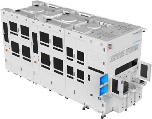
GeniusWay horizontal electroplating equipment serves as a core solution for advanced packaging, power devices, and compound semiconductor manufacturing, covering critical processes such as TSV, Pillar, Bump, and RDL to support chip miniaturization and high-performance enhancement.

Core Configurations

  • Compatible with 8–12 inch wafers
  • Supports multi-metal electroplating processes including Cu / Ni / Au / SnAg / NiFe
  • Supports up to 3 Load Ports
  • Configurable with up to 4 cleaning & drying chambers and 4 pretreatment chambers
  • Supports up to 16 electroplating chambers

Process Performance

Within-Wafer Uniformity
0 %
Wafer-to-Wafer Uniformity
0 %
Process Repeatability
0 %
核心优势
  • 实现高均匀性电场流场分布,优化晶圆边缘局部镀层厚度
  • 高深宽比 TSV/TGV 填充无空洞,保障镀层质量
  • 多腔体并行 + 连续传送设计,大幅提升批量生产效率
  • 模块化结构搭配密闭工艺腔,减少交叉污染,显著提高设备稼动率
工艺性能
  • 片内均匀性:<5%
  • 片间均匀性:<3%
  • 工艺重复性:<3%

Core Advantages

  • Achieves highly uniform electric field and flow field distribution, optimizing local plating thickness at wafer edges
  • Void-free filling for high aspect ratio TSV/TGV structures, ensuring plating quality
  • Multi-chamber parallel processing and continuous transfer design greatly improve mass production efficiency
  • Modular structure with sealed process chambers reduces cross-contamination and significantly improves equipment uptime
电镀的基本原理

Process Principle

Through direct current electrolysis, metal cations are reduced and deposited onto conductive substrates. The process offers extremely high deposition rates, excellent filling capability, and cost advantages through non-vacuum, non-high-temperature operation.
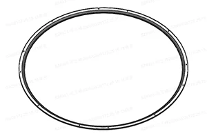
Key Components

Wafer Sealing Gasket
  • Application: Semiconductor wafer electroplating process sealing
  • Material: Perfluoropolymer material with excellent acid/alkali resistance and high-temperature resistance
  • Surface Treatment: Specialized anti-stick polymer coating to prevent wafer sticking
  • Service Life: ≥10,000 wafers per gasket
  • Advantages: Excellent chemical stability, long-lasting sealing performance, and yield protection
Elastic Conductive Ring
  • Application: Semiconductor wafer electroplating electrical conduction
  • Material: Precious metal-based material with superior conductivity
  • Structural Feature: Highly elastic design suitable for electroplating operations
  • Service Life: ≥10,000 wafers per ring
  • Advantages: Fully domestically developed and manufactured, long service life, and high stability
Wafer Support Ring
  • Application: Wafer support and positioning during semiconductor electroplating
  • Material: High-rigidity polymer material with excellent acid and alkali resistance
  • Process Feature: High-precision machining with excellent dimensional accuracy
  • Advantages: Fully domestically developed and manufactured, suitable for demanding electroplating environments
Electroplating Flow Distribution Plate
  • Application: Uniform flow distribution in semiconductor wafer electroplating
  • Material: Acid and alkali resistant polymer material with excellent chemical stability
  • Process Performance: High-precision machining with highly uniform flow guidance
  • Advantages: Fully domestically developed and manufactured, suitable for high-end electroplating equipment

Key Components

Wafer Sealing Gasket
  • Application: Semiconductor wafer electroplating process sealing
  • Material: Perfluoropolymer material with excellent acid/alkali resistance and high-temperature resistance
  • Surface Treatment: Specialized anti-stick polymer coating to prevent wafer sticking
  • Service Life: ≥10,000 wafers per gasket
  • Advantages: Excellent chemical stability, long-lasting sealing performance, and yield protection
弹性导电环
  • 应用场景: 半导体 Wafer 电镀制程导电
  • 核心材质: 贵金属基材,导电性能优异
  • 结构特性: 高弹性设计,适配电镀作业
  • 使用寿命: 单环适配晶圆数量≥10000PCS
  • 核心优势: 纯国产自主研发制造,长寿命、高稳定
晶圆支撑环
  • 应用场景: 半导体 Wafer 电镀制程支撑定位
  • 核心材质: 高刚性高分子材料,耐酸碱腐蚀、支撑稳固
  • 工艺特性: 高精度精密加工,尺寸精度优异
  • 核心优势: 纯国产自主研发制造,适配电镀严苛工况
电镀匀流板
  • 应用场景: 半导体 Wafer 电镀电匀流
  • 核心材质: 耐酸碱高分子材料,化学稳定性优异
  • 工艺性能: 高精度加工,高均匀导流
  • 核心优势: 纯国产自主研发制造,适配高端电镀设备